Timing Driven Placement: Optimizing Circuit Performance for Faster Speeds
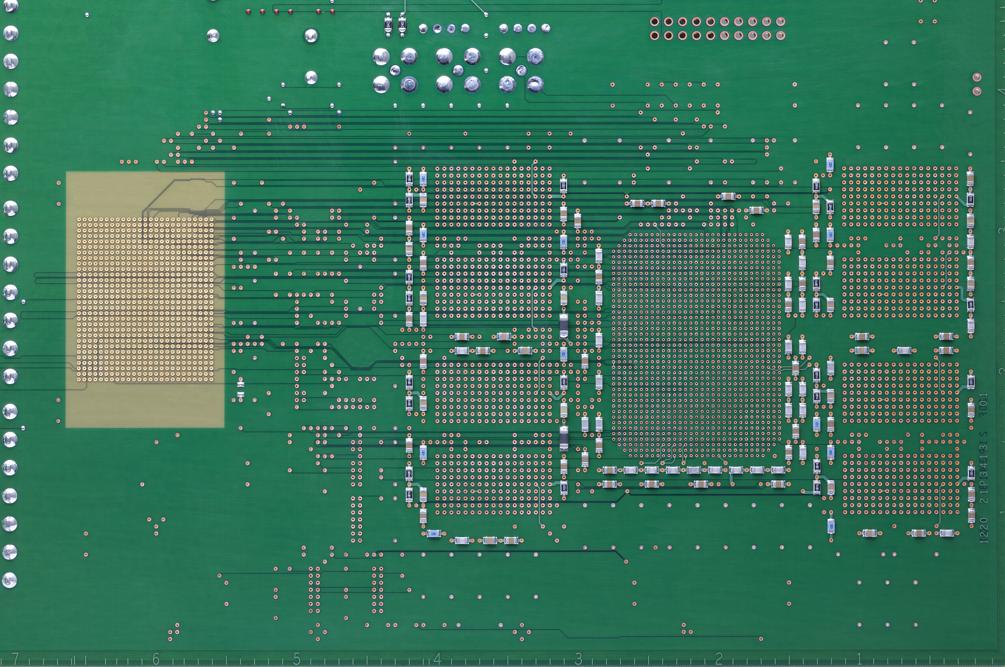
Timing driven placement is a technique used in electronic design automation (EDA) to optimize the layout of components on a printed circuit board (PCB) or an integrated circuit (IC) to meet timing requirements. The placement of components on a PCB or IC has a significant impact on the timing and performance of the circuit. In timing driven placement, the placement is guided by timing constraints, such as clock skew, maximum delay, and minimum delay. The goal is to minimize the delay between the components and ensure that the timing requirements are met. Timing driven placement is an important step in the physical design process of a circuit and is critical in achieving the desired performance and functionality of the circuit.

原文地址: https://www.cveoy.top/t/topic/lrxQ 著作权归作者所有。请勿转载和采集!