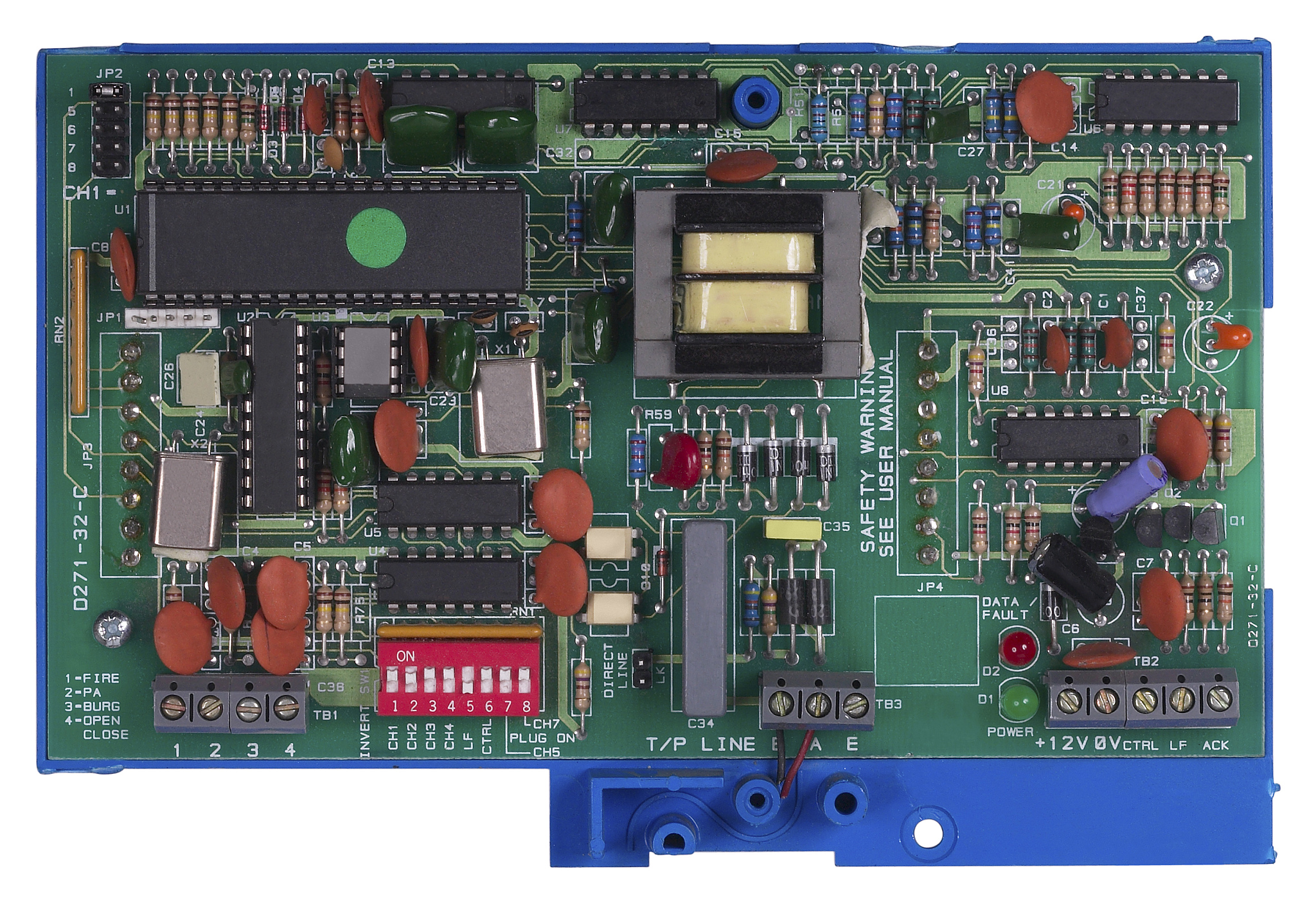
Timing Driven Placement: Optimizing PCB Design for Performance
Timing driven placement is a process of placing the electronic components of a circuit on a printed circuit board (PCB) in such a way that the timing requirements of the circuit are met. It involves using information about the timing constraints of the circuit, such as clock frequencies and delay requirements, to guide the placement of the components on the board. The goal of timing driven placement is to minimize the delay between components, which can improve the performance and reliability of the circuit. This process is typically performed by electronic design automation (EDA) software tools.

原文地址: https://www.cveoy.top/t/topic/lrx0 著作权归作者所有。请勿转载和采集!